VRAM
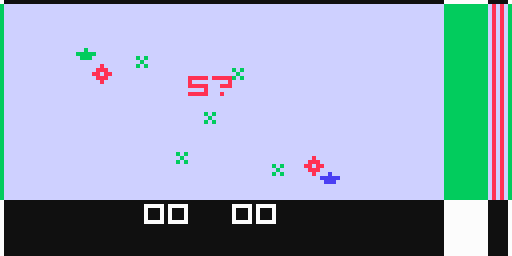
In the Channel F, VRAM is a 128x64 pixel ( 8192 x 2 bits / 2kByte ) portion of RAM in the console, that can only be accessed through the ports. A portion of this VRAM is used as the display on the television screen. Column 125 and 126 controls the palette for the row of VRAM it is written on. The rest of the VRAM is unused by the console, it can be written to but there's no way of reading it back, there's however Schach RAM available in some cases depending on your cartridge platform.
Regarding the hardware the DRAM is usually Fairchild's own with their own markings, it's an MK4027 compatible DRAM in the first generation of machines (a lot of logic chips) and a MK4015N compatible DRAM in the second generation (VLSI circuit). Good to know if you're looking for spare parts in case you have odd colored bars in your display.
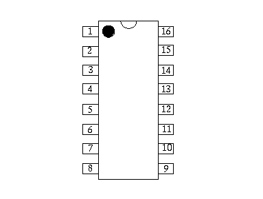
Pinout of the MK4027 and MK4015 (4096 bits) MK4027 datasheet, MK4015 datasheet:
1: -5V (Vbb)
2: Din
3: /Write Enable
4: /RAS
5: A0
6: A2
7: A1
8: +12V (Vgg)
9: +5V (Vdd)
10: A5
11: A4
12: A3
13: /Chip Select
14: Dout
15: /CAS
16: GND (Vss)
(Not sure about the difference between these, 4027 seems to be the sturdier alternative available in more speeds)
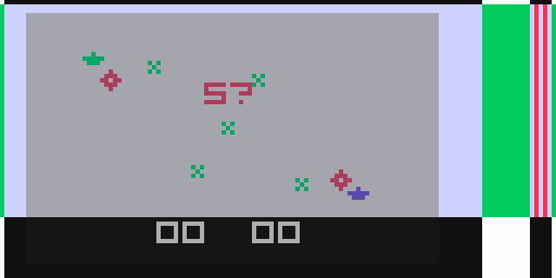
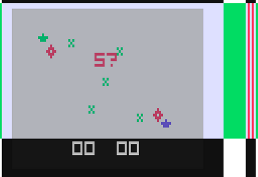
The portion of VRAM which is displayed starts at about column 4, row 4 and expands 102 pixels horizontally and 58 pixels vertically, giving a resolution of 102x58 pixels. This resolution is used in the MESS emulation system. However, most CRT televisions display a smaller resolution horizontally because of overscan, so the safe area to use is about 95x58 pixels. Many TV sets are adjusted wrong so that picture is offset in one or two directions. Zoomed and off center is what to normally expect, more or less. Note that the resolution is a lot closer to widescreen (16:9) than standard definition (4:3). On a TV from the 70's or 80's pixels are rectangular, standing on the short edge. In widescreen mode they are close to perfect squares.
Below is a screenshot showing visible and invisible portions of VRAM, taken by Sean Riddle using a modified version of the emulation system MESS.

Below is the same screenshot with the safe area marked, the portion of the screen that can safely be used for any TV.

This is the same image in the approximate aspect your TV will show it (only a few pixels past the safe area though).
Viewable area extends a few pixels past the safe area.

Other options
Video RAM has successfully been replaced with the slightly more modern 4164-15 DRAM chips, it needs pin 8 to be lifted and tied to pin 9 as it runs from +5V only and needs no +12V. The -5V on pin 1 is not connected on the 4164 chip so no change is needed there. Final change needed is a 1nF capacitor between Data out pin (pin 14) and ground (pin 16), possibly due to speed or different handling of the output.
Pinout and datasheet for the 4164:
1: Not Connected
2: Din
3: /Write Enable
4: /RAS
5: A0
6: A2
7: A1
8: +5V (Vcc)
9: A7
10: A5
11: A4
12: A3
13: A6
14: Dout (Q)
15: /CAS
16: GND (Vss)
As can be seen the 4164 is a 64kbit chip, when used in the System Fairchild unit A7 is held high as it's connected to +5V and A6 is held low as /Chip Select is tied to ground.
I recommend using 4027 if available. /e5frog
